The ASIC flow uses open tools and open PDKs only. It is verified on Linux with Yosys, OpenROAD, KLayout 0.28 and 0.30, Magic 8.3.465 and netgen 1.5.272, on the test designs and the example chips named below. It has not been run on Windows, and not on a customer design. A design at realistic size can exceed the build machine's memory: KLayout's GDS step stopped at 11.8 GB on a core of about 10,000 cells on GF180MCU.
Requirements
- Yosys, OpenROAD and KLayout (0.30 for the PDKs' current DRC and LVS decks). For SKY130 sign-off LVS, Magic (8.3.411 or newer for the PDK tested) and netgen.
- The PDKs in the open_pdks layout that volare and ciel install, under
PDK_ROOTorneuralInverse.hdl.asic.pdkRoot.
Supported PDKs
PDK (pdk) | Standard cell libraries (library) | Supply (voltage) | Pad ring (pads, padDrive) |
|---|---|---|---|
ihp-sg13g2 | sg13g2_stdcell | 1.2 V | Yes: sg13g2_io, 4 (default), 16 or 30 mA |
sky130A | sky130_fd_sc_hd (default), _hdll, _hs, _ms, _ls | 1.8 V | No |
gf180mcuD | gf180mcu_fd_sc_mcu7t5v0 (default), gf180mcu_fd_sc_mcu9t5v0 | 5 V (default) or 3.3 V | Yes: gf180mcu_fd_io, 4 (default), 8, 12, 16 or 24 mA |
Describe a chip
Add the chip to the asic list of hdl.json:
"asic": [
  { "name": "core_ihp_sg13g2", "pdk": "ihp-sg13g2", "top": "monitor_core", "clock": "clk", "period": 25, "pads": true, "padDrive": 4 },
  { "name": "core_sky130", "pdk": "sky130A", "library": "sky130_fd_sc_hd", "top": "monitor_core", "clock": "clk", "period": 25,
    "activity": { "testbench": "adc_monitor_tb", "instance": "adc_monitor_tb.dut.u_core" } }
]
Each chip has its pdk, top unit, clock port and period (ns), core utilization and aspectRatio, optionally a library and voltage, pads and padDrive for a pad ring, activity for power from simulation, and its own SDC file in constraints when the default constraints are not enough.
Build it
- Run Open Chip (RTL to GDS) and pick the chip.
- In the Chip editor, run Build RTL to GDS.
The flow: Yosys maps the design to the PDK's standard cells; OpenROAD floorplans, places, builds the power grid and clock tree, repairs timing, routes and fills; KLayout writes the GDS and runs the PDK's DRC deck (neuralInverse.hdl.asic.drc, default on) and LVS deck (neuralInverse.hdl.asic.lvs, default on). On SKY130, LVS uses the PDK's own Magic and netgen sign-off flow when they are installed. Sign-off follows: parasitic extraction, antenna checks, IR drop per supply, timing at each of the PDK's corners with extracted parasitics, and crosstalk.
The Chip editor shows the worst setup and hold slack, the cells, area and utilisation, power at the typical corner, what the router could not fix, whether the layout matches the netlist, antenna violations, IR drop, each corner's paths with and without crosstalk, and the DRC violations by rule, each leading to its place in the layout. A failing step is reported with its last lines and the step of the flow it reached. From the Chip editor you also open the timing reports, the netlist, the OpenROAD script and the layout, and draw any corner's setup or hold path in the layout.
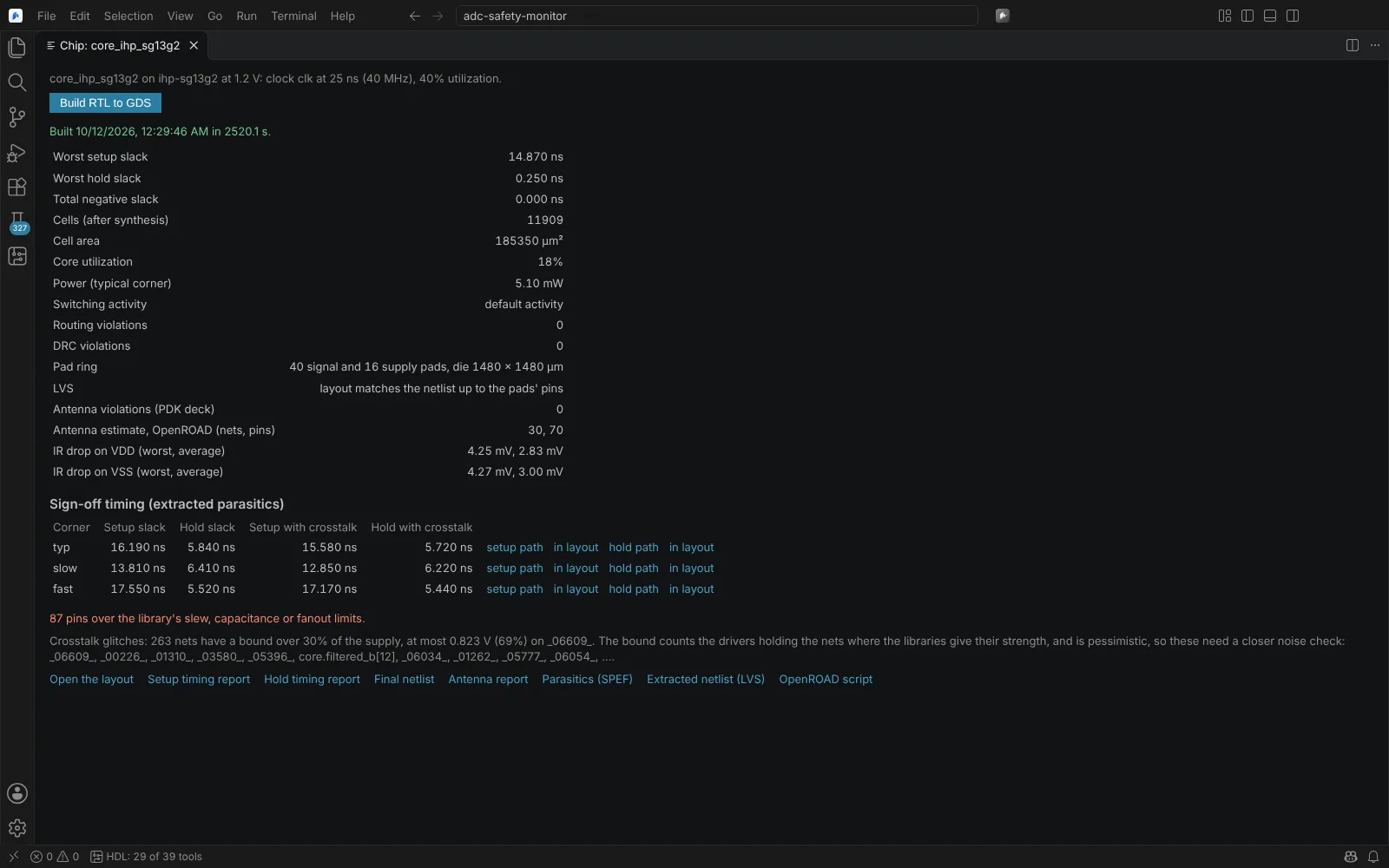 The Chip editor for a core with a pad ring on IHP SG13G2: slack, cells, power, DRC, LVS, antennas, IR drop and sign-off timing per corner
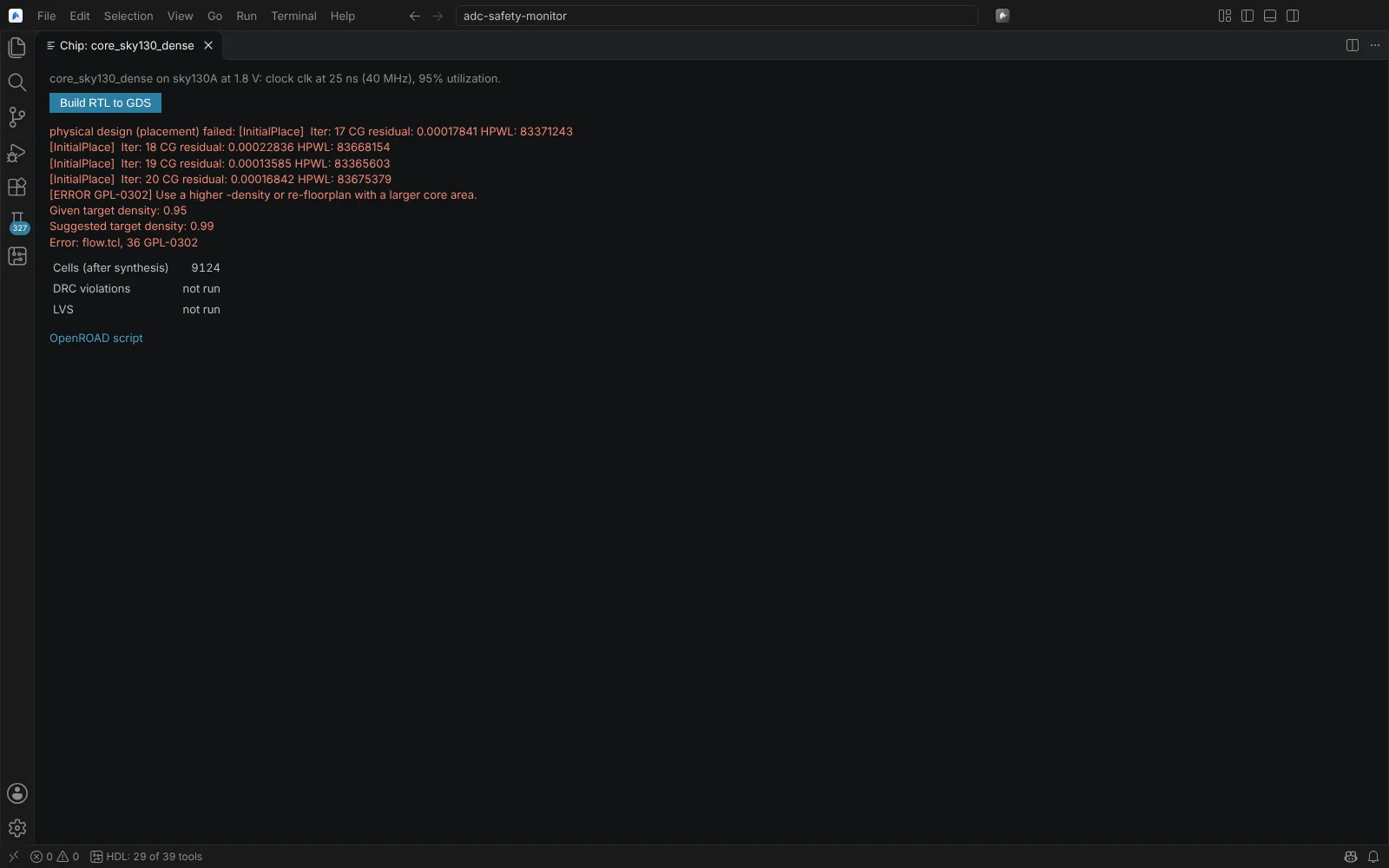 A failed placement step reported in the Chip editor with the tool's last lines
What was verified: a counter built to GDS with each of the eight libraries (GF180MCU at both supplies), and with a pad ring on IHP SG13G2, DRC clean and LVS matching where it runs, no antenna violation, timing met at every corner. On the ADC monitor example: monitor_core on IHP SG13G2 with a pad ring and on SKY130, and safety_monitor on GF180MCU, timing met, DRC clean, LVS matching. On SKY130 the example has 7 nets over the antenna rules.
Our crosstalk glitch bound and IR drop figures are screens, not foundry sign-off; treat them as such.
Layout viewer
GDSII and OASIS files open in the Layout Viewer, read by our own code: cells on their layers in the PDK's colours (from its KLayout layer properties), layers shown and hidden, zoom about the cursor (wheel, +/-), pan (drag, arrows), fit (F), the cursor's place in micrometres, the top cell to show when there are several, cells too small to see drawn as outlines, the top cell's pin labels, KLayout DRC violations marked and listed, and a timing path from the Chip editor drawn through its cells. Verified against KLayout on the flow's GDS and OASIS output.
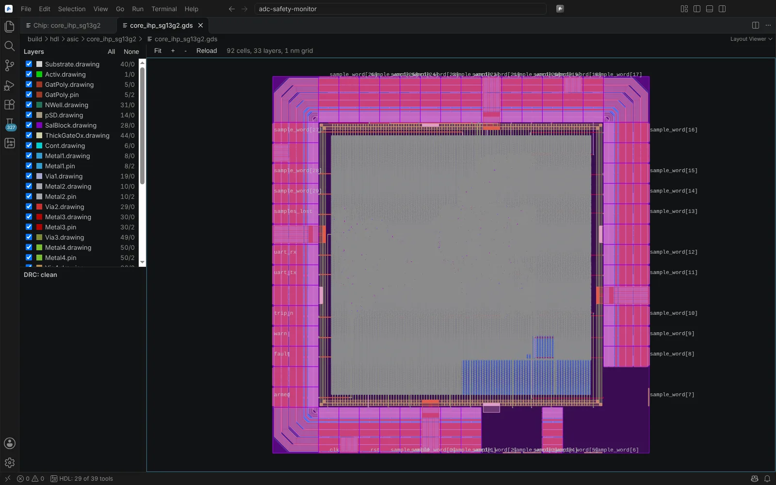 A chip's GDS with its pad ring in the Layout Viewer, layers listed and DRC clean
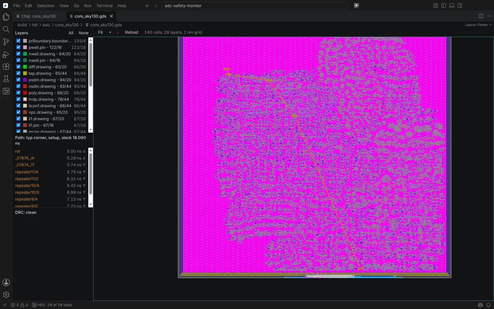 A timing path from the Chip editor drawn through its cells on a SKY130 layout
Power from simulation
A chip (or a Vivado target) can name a testbench in activity (testbench, and optionally instance, waveform, start and end in ns). The build runs the testbench, reads its VCD or FST, and writes SAIF 2.0 for the power analysis. The Chip editor says which activity the power was worked out with. Verified with Icarus Verilog, GHDL and OpenSTA through OpenROAD; Vivado's read_saif is modelled.
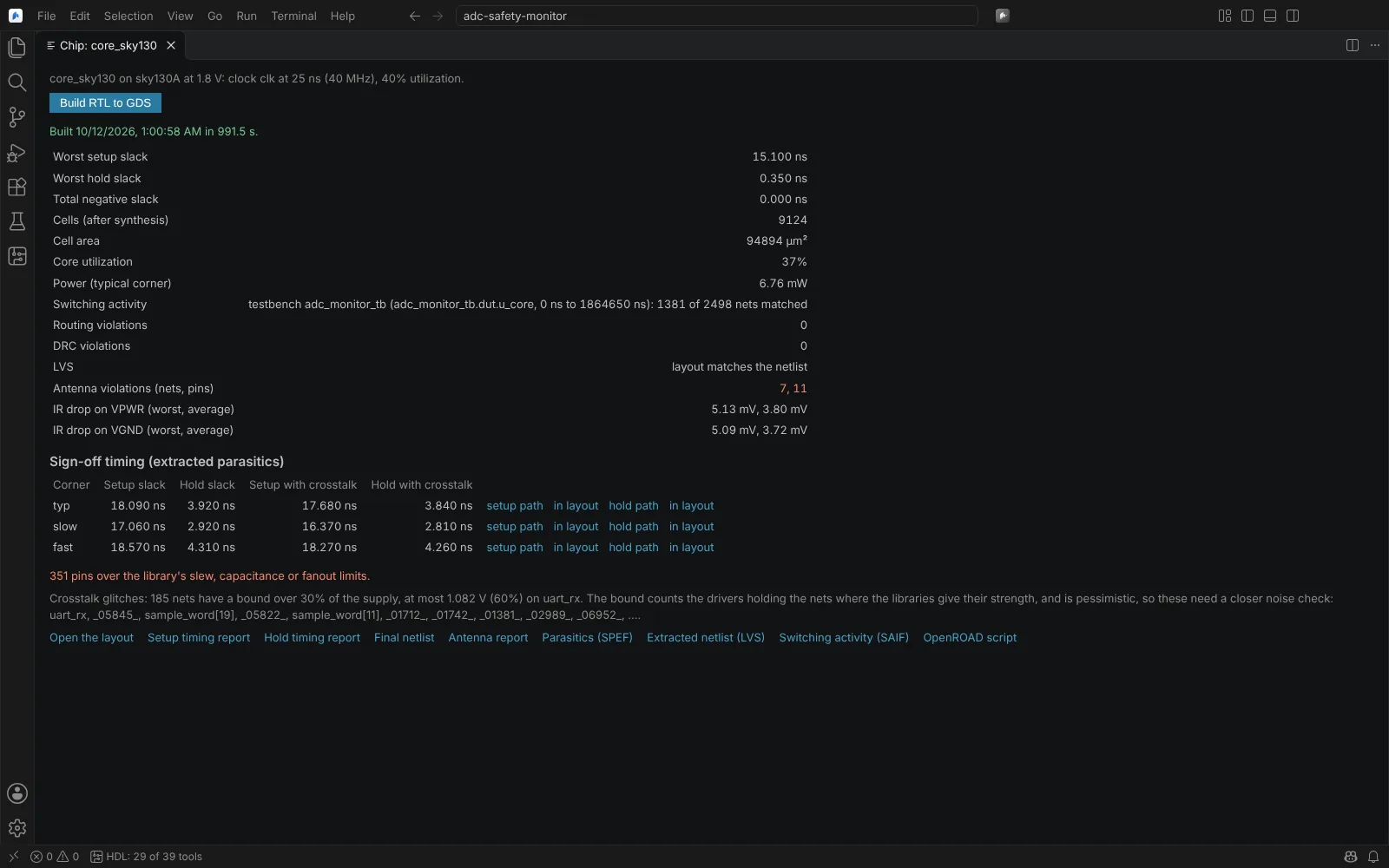 A SKY130 chip whose power was worked out from the system testbench's switching activity